Which industries are applicable to semiconductor device testing?
Semiconductor device testing is used in many semiconductor industries. So, how much do you know about semiconductors and conductors for semiconductor device testing? The properties of this substance are still recommended to the user.
In general, substances can be classified into conductors, insulators, and semiconductors according to their electrical conductivity. The conductive properties of a substance depend on the atomic structure. Conductors are generally low-cost elements, such as copper, iron, aluminum and other metals, the outer electrons of which are bound by the nucleus are very small, so they easily break away from the nucleus and become free electrons. Therefore, under the action of an external electric field, these electrons generate directional motion (called drift motion) to form a current, which exhibits better electrical conductivity. The electrons of high-priced elements (such as inert gases) and high-molecular substances (such as rubber and plastics) are strongly bound by the nucleus. They are not easily detached from the nucleus and become free electrons. Therefore, they are poorly conductive and can be used as insulating materials. The outer electrons of semiconductor materials are not as easy to get rid of the nucleus as the conductors, become free electrons, and are not as tightly bound by the nucleus as insulators. Therefore, the conductive properties of semiconductors are somewhere in between.
A semiconductor with a pure crystal structure is called an intrinsic semiconductor. Commonly used semiconductor materials are silicon and germanium, which are tetravalent elements with four valence electrons in the outer orbital of the atomic structure. When a silicon or germanium material is drawn into a single crystal, a pair of outer electrons (valence electrons) of two adjacent atoms become a common electron, which on the one hand moves around their own nucleus and on the other hand appears in the orbit to which the adjacent atom belongs. on. Immediate electrons are not only affected by their own nucleus, but also by adjacent nuclei. Thus, two adjacent atoms share a pair of valence electrons to form a covalent bond structure. Therefore, in the crystal, each atom is closely related to the surrounding four atoms by covalent bonds.
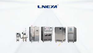
LNEYA semiconductor device testing is widely used in high and low temperature testing of semiconductor equipment, electronic equipment high temperature and low temperature constant temperature testing cold and heat source, the semiconductor testing industry is used more.
(Content source network, if there is any infringement, please contact to delete.)
Related recommendations
-
Temperature requirements for ion implantation chillers in semiconductor manufacturing processes
1296Ion implantation is an important step in semiconductor manufacturing processes to precisely dope and control the electrical properties of semiconductor materials by implanting high-energy ions into them. This process generates a lot of hea...
View details -
Rotary shaft freezing process in new energy automobile motor assembly
1883As the market for new energy vehicles has gradually expanded, the new energy motor manufacturing industry has also grown. Then, for the motor manufacturer, the rotor into the core process during the motor assembly process is particularly important...
View details -
When to choose TCU temperature control system?
1547First of all, we need to know that the reaction kettle generally needs to carry out the necessary temperature control along with the chemical reaction of the material itself. Through the temperature change of the circulating medium in the jacket ...
View details -
From what aspects should we consider the use of circulating coolers?
1387Circulating coolers are a popular choice for temperature-critical applications because they provide stable temperature control, constant flow and constant pressure control. Many process heating systems require cooling and heating. For example, man...
View details
 LNEYA Industrial Chillers Manufacturer Supplier


