Cooling and heating system TES for integrated circuit wafer cooling method
Integrated circuit products have been developed for more than 50 years and are the most advanced high-tech industries. Integrated circuit or chip / chip. The complete chip manufacturing process includes chip design, wafer manufacturing, package manufacturing, and testing. The wafer manufacturing process is particularly complicated.
The raw material of the chip is silicon, and the silicon is refined by quartz sand. The wafer is purified by silicon (99.999%), and then these pure silicon are made into silicon ingots, which are used to manufacture integrated circuits. The material of a quartz semiconductor is sliced into wafers specifically needed for chip making. The thinner the wafer, the lower the production cost, but the higher the process requirements.
After the wafer is processed, an important process index that needs to be achieved is that the particle size cannot exceed the standard. It is necessary to strictly control the cleanliness of the entire equipment structure and minimize mechanical friction. In order to prevent friction during wafer transfer, on the one hand, it is necessary to ensure that the transmission conditions such as wafer cooling temperature and cooling air flow reach the normal working range of fetching.
—General wafer transfer can be carried out under conditions where the wafer temperature is <50°C. After the wafer is processed, when the boat is lowered from the furnace tube to the wafer carrying area, a wafer cooling step is also required to reduce the deformation of the wafer and meet the transfer conditions.
Existing wafer cooling methods generally set the flow of nitrogen gas in the process of lowering the boat according to the LPCVD and low temperature annealing process conditions that require high oxygen content in the wafer carrying area. Specifically, the nitrogen flow rate into the wafer carrying area is set to the maximum, and the wind speed of the cooling fan is adjusted to a high level. On the premise of ensuring that the oxygen content reaches the standard, the wafer is continuously cooled until it passes the detection device. It was detected that the cooling state of the wafer reached the transfer condition of the robot. The disadvantage of this cooling method is that on the one hand, during the cooling process, when the oxygen content reaches the control target, the set nitrogen flow rate and cooling air speed are not changed, resulting in excessive nitrogen consumption, especially for the oxidation process, which affects the wafer The requirement for oxygen content in the load-bearing area is not high, which increases the consumption of nitrogen. On the other hand, the cooling conditions have not been reasonably adjusted according to the characteristics of various parameters affecting the cooling time. Without control, its actual cooling efficiency is low, which adversely affects wafer throughput.
Realizing effective control of wafer cooling during the process of lowering the boat can quickly and effectively reduce the temperature of the wafer and shorten the cooling time, thereby increasing wafer production capacity and significantly saving nitrogen resources as a cooling medium.
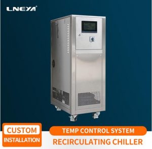
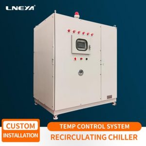
TES Series-Cooling Heating System
LNEYA stands for international advanced liquid temperature control technology. It actively explores and researches component test systems. It is mainly used for temperature test simulation in semiconductor testing. It has wide temperature orientation and high temperature rise and fall, which solves the problem of temperature control lag in electronic components.
This product is suitable for precise temperature control of electronic components. Temperature control range: -85° C ~ 250°C; Power range: 2.5kW ~ 25kW; Temperature control accuracy: ± 0.3°C. Ultra-high temperature cooling technology can directly cool from 300°C. In the manufacture of semiconductor electronic components used in harsh environments, the assembly of IC packages, as well as engineering and production test phases include electronic thermal testing and other environmental test simulations at temperatures (-85°C to + 250°C). Once put into practical use, these semiconductor devices and electronics can be exposed to extreme environmental conditions to meet stringent military and telecommunications reliability standards.
Pipeline LNEYA’s TES series equipment to the chip test fixture stand. The cooling and heating system TES equipment runs through its own liquid medium, provides the required temperature to the test bench through the input and output pipes, and takes the heat of the tested chip back to the TES equipment for recycling, which not only has a high reuse rate but also saves testing costs. It solves the indispensable nitrogen consumption problem in the existing cooling technology mentioned above, and also solves the safety and temperature control accuracy.
Related recommendations
-
How to choose a heating and cooling circulating water bath?
1334Heating and recirculating water bath In the process of selection, heating power, cooling power, pressure and flow are also factors that users need to consider. Good system design and accessory brand selection are related to the whole heating and c...
View details -
What should I pay attention to when adding refrigerant to a water-cooled chiller
1124In our life, we believe that everyone isvery familiar with refrigeration. In the central air conditioning andindustrial production process cooling industry, small water-cooled chillers ismore common. This unit is composed of a compressor in the...
View details -
Application of Microchannel Reactor Temperature Control System in the Laboratory
875Application of Microchannel Reactor Temperature Control System
View details -
Solution to the inability to cool down the industrial high and low temperature recirculating chiller
1146When the high and low temperaturerecirculation chiller system is in use, what is the general cause if the hightemperature cannot be reduced? How should we deal with such failures?First, let’s analyze theprinciple and method of cooling. The circ...
View details
 LNEYA Industrial Chillers Manufacturer Supplier


